How Chemical Etching Could Advance 5G Technology
April 2021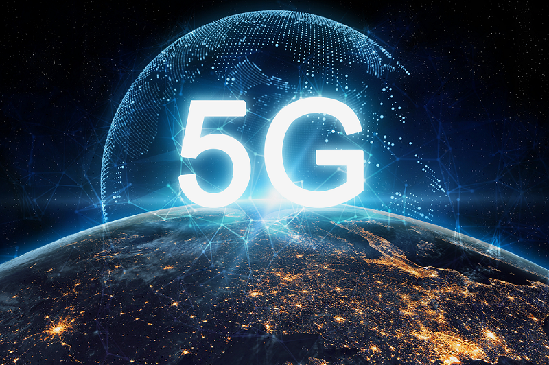
The advent of 5G technology has inspired a lot of discussion in the news, mostly centering on the ways it promises to improve cellular communications. While 5G will certainly enhance the technology used to power cell phones, its potential range of innovation extends well beyond just that.
Over the next few years, the power of 5G will make itself felt across multiple industries and in many areas of our lives. Chemical etching will play a major role in the development of devices and systems that rely on 5G technology. What follows is a brief overview of 5G and its still-evolving relationship to chemical etching.
5G: The Basics
5G, which stands for “fifth generation,” is the next stage in the development of telecommunications technology. It should be thought of as a technology standard rather than a specific type of technology. Introduced in 2016, 5G has been rolled out slowly, and it has yet to complete the process of supplanting the older 4G standard. It’s important to understand that 5G is not merely a more advanced version of 4G; it is, in fact, based on innovations that constitute a huge leap over its predecessor and should stimulate large-scale improvements in the Internet of Things (IoT).
5G frequencies can be classified into three separate groupings. Broadly speaking, these groupings can be defined as follows:
- Low-band: This includes frequencies below 1 GHz.
- Mid-band (Sub-6): This includes frequencies between 3.6 GHz and 6 GHz.
- High-band (mmWave): This includes frequencies between 24 GHz and 40 GHz. 1
The traditional 4G spectrum utilizes low-band frequencies. By contrast, 5G will be able to operate in the Sub-6 and mmWave frequencies.
How do the two types of frequencies compare? Sub-6 can provide greater geographical coverage, but mmWave offers improved downlink speeds. It’s also worth pointing out that mmWave frequencies tend to have difficulty with obstructions—they can be blocked by buildings and even the hand of an individual holding a smartphone. This is a challenge that manufacturers of 5G-compliant technology must grapple with.
Network carriers are expected to offer a combination of Sub-6 and mmWave services to provide optimal speed and coverage.
Benefits of 5G
5G offers a number of improvements over traditional 4G technology, including:
- Speed – 5G is twenty times faster than 4G.2
- Greater bandwidth – 5G can connect to more devices, which means more reliable access to services.
- Lower latency – 5G reduces the time needed for transmitted information to receive a network response.
The improved speed and data delivery capacity of 5G will markedly improve many vital services. Self-driving cars will rely on 5G to improve reaction times and avoid accidents. First responders will be able to react more quickly to emergency situations. In addition, the general public will be able to benefit from faster video streaming and improved cell phone performance and capacity. These are only a few technological improvements we can expect from 5G.

The Role of Chemical Etching
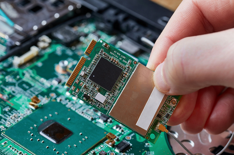
How does photo chemical etching factor into the 5G revolution? It will play a vital role in the manufacture of technology needed to handle 5G frequencies. Standard 4G circuit boards simply aren’t adequate for the speed and bandwidth requirements of 5G; therefore, it is necessary to devise PCBs that can manage these demands. 5G will require much stricter attention to impedance control and the mitigation of signal loss. This in turn requires the kind of extreme precision of design that photo chemical etching can provide.
Unlike laser cutting and alternative fabrication methods, chemical etching does not inflict distorting stresses on the material—a benefit that becomes increasingly important as PCB components become tinier and less forgiving of imperfections. Chemical etching also carries the manufacturing advantage of accommodating production runs of virtually any size.
Chemical etching has already had a substantial influence on the miniaturization of electronic devices and the development of high-density interconnect (HDI) circuit boards. Chemically etched HDI boards have enabled manufacturers to create circuit boards with a significantly higher wiring density per area, leading to the development of faster, smaller products.
More recently, the development of a modified semi-additive process (mSAP) holds enormous promise as an aid in the creation of highly precise 5G-standard components. As its full name implies, mSAP differs somewhat from conventional chemical etching processes, which are subtractive in nature. Rather than subtracting material via etching, mSAP adds a thin copper foil layer to the photoresist. This copper etching process enables the formation of extremely precise, “clean” straight lines and greater circuit density.
The process is widely used in integrated circuit substrates, and its prevalence in the technological sector is sure to increase in the coming years.
Headquartered in Camarillo, CA, United Western Enterprises draws upon decades of experience to provide clients across a wide range of industries—from the aerospace sector to the automotive fields—with high-quality photo-etched parts and components. UWE, Inc., is an AS 9100D / ISO 9001:2015 Certified Company. For more information about our services, call 800-964-6461 or contact us online at your convenience.
Sources