Advantages of Photo Chemical Etching
Photo-etching is a chemical milling process. Otherwise known as photo chemical machining (PCM), it is used to fabricate sheet metal components and is an alternative to laser cutting, metal stamping, electric discharge machining (EDM), and waterjet cutting. Photo-etched parts can be produced accurately and economically compared to using other methods.
The process of photo-etching emerged in the early days of the printed circuit board industry. It has grown in popularity since its emergence in the 1960s. Suited for materials with metal thicknesses of 0.0005 to 0.080 inches, or 0.013 to 2.032 millimeters, it can be applied to cutting any metal or alloy on the commercial market. That includes aluminum, steel, stainless steel, brass, titanium, nickel, and silver.
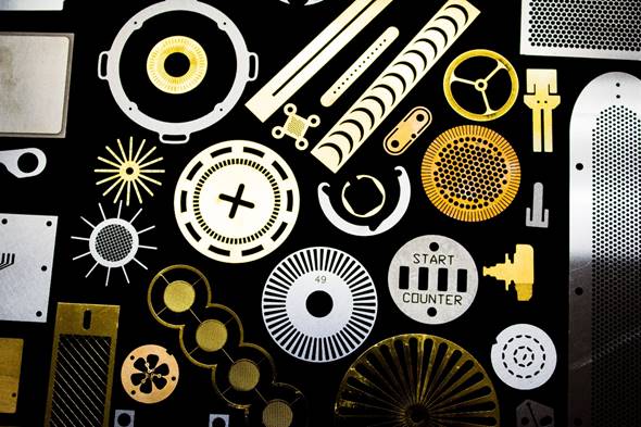
Photo-etching is ideal for creating the following parts in industrial settings:
- Fine screens and meshes
- Metal gaskets/seals
- Heat sinks
- Sensors
- Springs
- Circuit components
- Flexible heating elements
- Electrical contacts
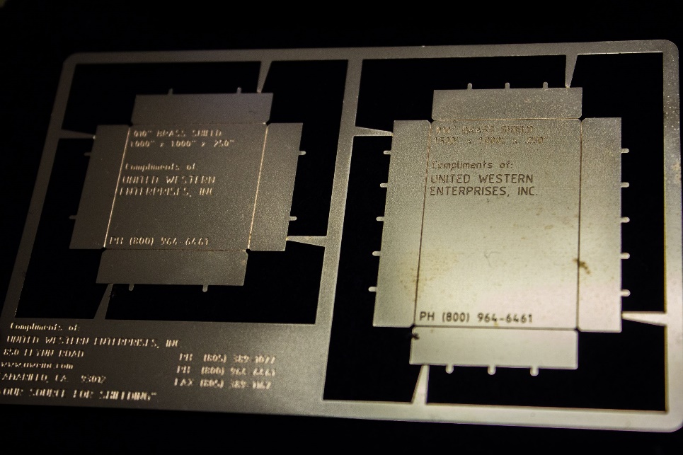
- EMI/RFI shields
- Jewelry
The Photo Etching Process
Numerous metal types can be photo etched, allowing for a large array of material options to be available for customer orders. On new orders, the process begins with material selection based on customer requirements. Utilizing the customer design, a tool is created by printing the design onto a photographic film. This dimensionally stable, clear photo tool has two sheets (forming the top and bottom halves of the tool), which consists of negative images. Black areas are the sections that are etched while the clear shapes are the parts to be made.
The next phases of etching precision metal parts are as follows:
- Cutting: Raw material is cut to size based on process requirements.
- Cleaning: The metal sheets are cleaned before any processing can proceed. To properly clean them, chemicals are used to remove not only debris but also oils and waxes. Degreasing yields a contaminant-free surface to work with.
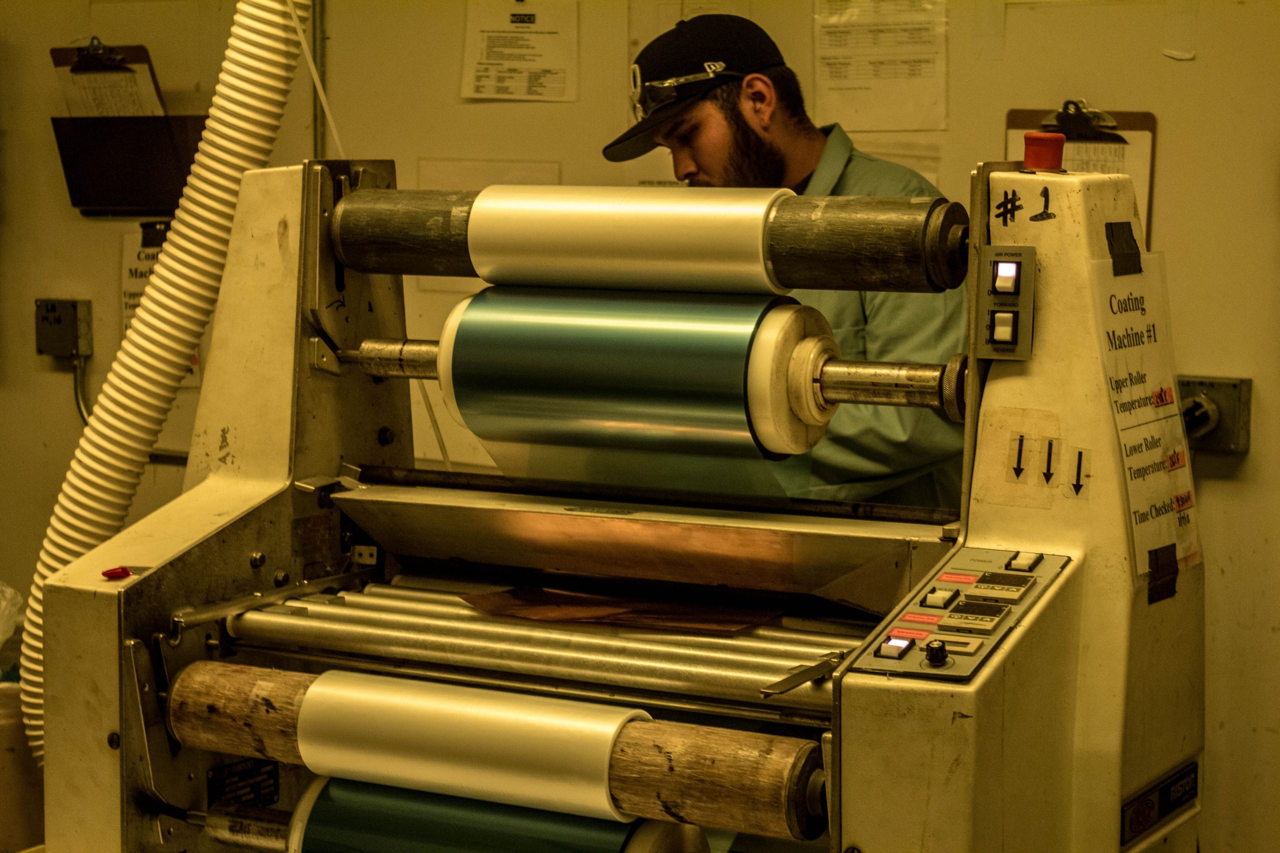
- Coating: In an ultra-clean environment, a photo-sensitive resist is added to the metal. The resist maximizes accuracy, repeatability, and the quality of the final product. An automated process is used to coat the material.
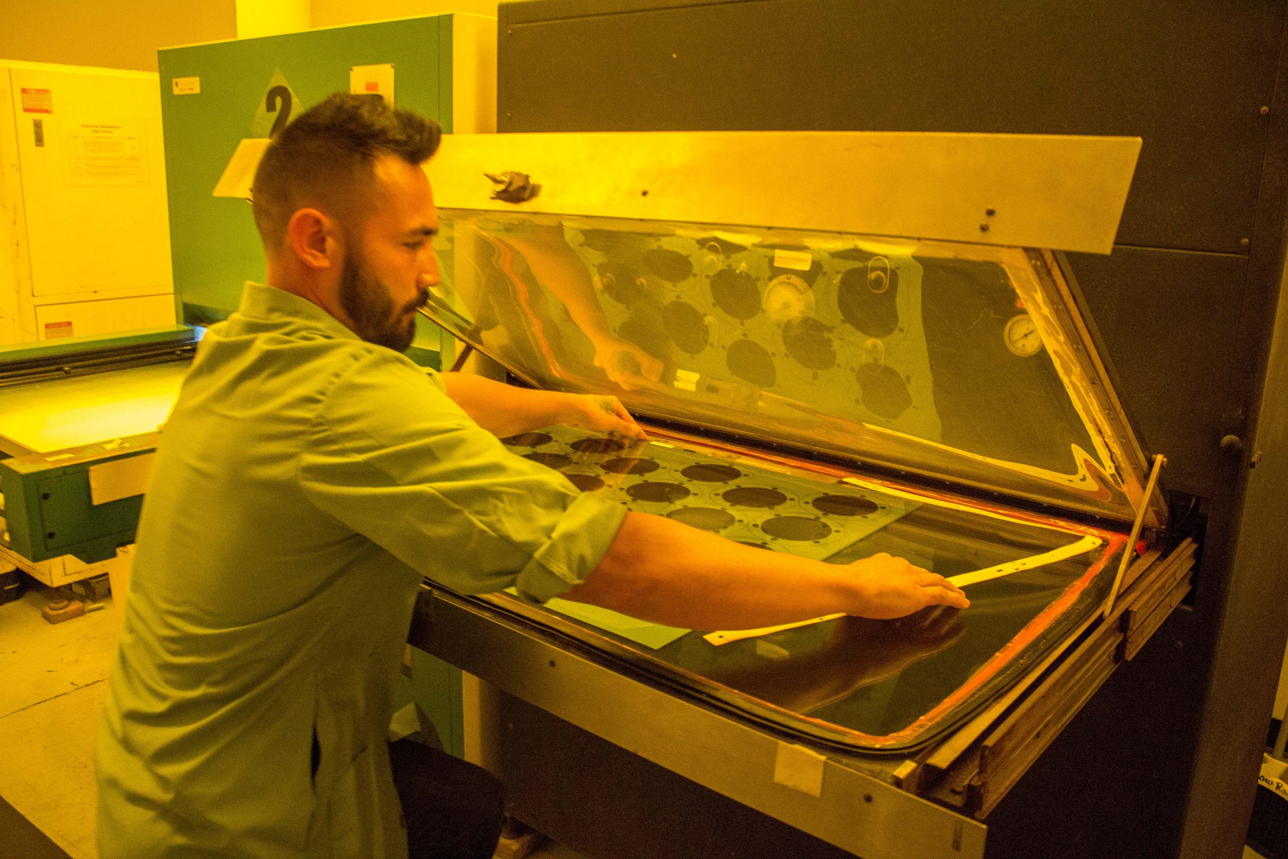
- Printing: Coated material sheets are then placed between the two photo tool sheets; contact between the photo tool and metal plate is optimized by a vacuum. A UV light is applied to the sheets where the exposed area hardens and the area unaffected by light remains soft.
- Developing: Next, the printed sheets can be developed by washing away the soft unexposed resist. Areas where resist was exposed remain protected and will keep the underlying material intact during the etching process.
- Etching: Sheets are now ready to be processed using chemicals essential to the etching process. The acidic solution utilized is heated and pressurized, reacting with exposed, unprotected metal surfaces, effectively eroding them away and leaving behind the parts from the original photographic film.
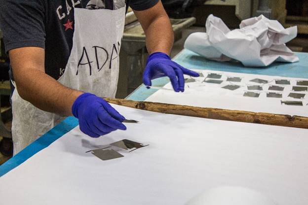
Post etching processes include neutralizing the acid and rinsing the sheet. Remaining photo-resist is removed so the photo-etched parts are produced in full form. After the resist is stripped, the parts are cleaned, dried, and inspected. A visual examination is performed, and a dimensional inspection is completed using specialized metrology equipment. Forming, polishing, bonding, plating, and other finishing steps may follow in the last stage of the photo etching process.
Advantages of Photo Etching over Other Methods
Suited for creating complex shapes and patterns with high precision, photo etching is highly advantageous over other manufacturing methods, including:
- Laser Cutting: High-powered lasers and advanced optics are effective in cutting materials. Some advantages include no direct contact between the tool and material, limiting the risk of accidental marking and cutting. However, this method is cost-effective only for small volume production. Laser cutting is too expensive for mass production and multiple parts cannot be made simultaneously, as with photo etching.
- Metal Stamping: Flat sheet metal is inserted into a stamping press. It is then formed into the desired shape by a tool and die surface. The tools are comparatively expensive, although effective for miniaturization. However, chemical etching is ultra-precise and a more affordable and less time-consuming process, even compared to micro-stamping. With stamping, just preparing the tooling can take 6-8 weeks.1 Photo-etching tooling can be created in a matter of hours.
- CNC Machining: The tools associated with Computer Numerical Control Machining require a significant investment. Small production volumes are not cost-effective and, even in higher volumes, the long-term costs (for production and maintenance) are higher than with chemical etching. Photo chemical machining enables the production of thousands of parts without additional tooling.
- EDM: With Electrical Discharge Machining, a part is created by removing materials using sparks or strong electrical discharges. It’s as cost-effective as photo etching for small volumes or producing prototypes. Etching, however, is a more cost-efficient process for large-scale, industrial production.
- Water Jetting: High-pressure water jets, sometimes mixed with abrasives, can cut various types of materials when focused into a narrow beam, including metal. The operation costs are high. Comparatively, chemical etching is the more affordable option when it comes to prototyping, small volume, or large volume production.
Photo-etching is not only precise and cost-effective for creating precision metal parts, it is also more flexible. The design flexibility is much greater than with other methods requiring expensive tooling adaptations for the slightest change. Companies might only pay a couple hundred dollars for a design change, without a significant increase in lead time. This makes chemical etching desirable for prototyping and full-scale production.
Stamping leaves burrs along the edges of metal, which need to be removed during another step in the manufacturing process. Photo-etching does not produce burrs, and it eliminates the need for deburring, which involves cost and time. The elimination of production steps also reduces lead time, so companies, therefore, receive component orders in a much shorter timeframe.
Batch size and part complexity also influence which method to use. At part thicknesses of 0.5 millimeters, wire EDM is suited for low batch sizes and stamping for higher production volumes, with photo etching falling in the middle. At 2-millimeter thicknesses, photo etching becomes more practical the more complex a part is, at high volumes. All areas of a part are etched at the same time, making the process more favorable than other methods when producing highly complex parts.
Maximizing the Benefits of Photo Etching
Producing photo-etched parts is fastest with lower-range thicknesses. The thicker a part, the more time it takes to etch through it (for most alloys, the etch rate is from 0.0005 to 0.001 inches per minute, on each side2). So, to maximize the benefits, you might limit production to thinner components. This is fine if your application only requires parts of this scale.
Photo-etching is also beneficial because it does not impose thermal stress on a material, as laser cutting does; no metal, regardless of its hardness, ductility, or grain structure, undergoes changes to its properties.
Exposed only to light, photo tools do not wear out like more traditional tools. Stamping and punching dies wear significantly with use. Chemical etching is the way to go if producing complex, fragile components such as semiconductor lead frames. Producing millions of these demands a process as effective as photo etching.
To make the process even more cost-effective, one can try fitting as many precision metal parts as possible on a sheet, which is the primary unit of labor compared to larger, wear-prone, expensive tools used with other production methods.
The sheet plan and size, however, must be consistent with each part’s size and dimensional tolerances. Design flexibility and expertise enable a high number of parts per sheet, further lowering the unit labor cost per individual component.
In short, photo etching is:
- Fast
- Precise
- Low cost
- Flexible
- Stress-free
- Burr-free
Thus, it is used for a wide range of industrial applications, from fine screens and meshes to RF and microwave circuits and their components, to fuel cell components. Photo-chemical milling is used for producing parts in aerospace, medical, telecom, and defense industries, or anywhere thin metal parts are used.
United Western Enterprises, Inc. produces photo-etched parts for a diverse range of clients. Combining computer-aided design, photography, chemistry, and metallurgy, the process can yield thin metal parts in a short time, with precision and cost-effectiveness. Parts can be manufactured to the customer’s specifications; these include:
- Shielding
- Shims
- Apertures
- Encoder disks
- Fine screens
- Battery contacts
- Covers and lids
In addition to the typical applications, we can also produce custom parts. Our precision involves tight tolerances; for instance, fine screens requiring small openings can have holes down to .012 inches in diameter (assuming a .010 thick screen), while encoder disks .005 inches thick can feature webs down to .004 inches. The slots can be as little as 1.2 times the thickness of the metal etched.
Our processes add even more advantages to photo etching, so the precision metal parts created have even more value. In addition to greater precision and value-added services, these advantages include:
- Support for 0.0003- to 0.063-inch metal thicknesses.
- Low tooling cost
- Fast turnaround
- Repeatability
- Burr-free, complex parts
UWE also offers:
- Anodizing
- Black oxide finishing
- Heat treatment
- Painting
- In-House forming
- Plating
- Laser welding
Once parts are created, we weld any seams shut and solder open seams. Plating on brass and steel parts enables us to solder components to boards and protect base materials from oxidation. A range of other beneficial services can be added to maximize the advantages and versatility of components. This results in precision metal parts ready for use in our customers’ applications.
We are also flexible in terms of thickness. In addition to the standard tolerances, UWE can produce parts up to .090 inches thick, and we have performed partial etching or engraving of material up to .250 inches thick. Other dimensions and tolerances depend on the thickness and nature of the part.
Do you have any questions or require photo-etched parts with tight tolerances, of extremely high quality? Contact United Western Enterprises, Inc. to request a quote or information; or request a call from us today. To reach us directly, call (800) 964-6461 or email sales@uweinc.com.
Sources